半导体
现代电子工业使用各种半导体材料。晶体管、太阳能电池和发光二极管等尖端器件,将自身的材料性能推向极致,并且需要非常均匀一致的源材料。拉曼光谱是研究半导体的理想工具。
表征半导体
您可以使用拉曼对所有半导体(例如Si、碳基材料、III-V族,及聚合物)和超导体进行表征和成像。拉曼分析可揭示许多信息,包括:
- 化学构成(例如,半导体化合物的合金片段)
- 多型体(例如,4H-SiC和6H-SiC)
- 应变/应力
- 掺杂浓度
- 薄膜厚度
- 晶体结构的类型和取向
- 晶体质量
- 均匀度和纯度
- 器件温度

分析简单
拉曼分析简单易行,因为无需样品制备。它不需要真空技术,也不会受到使用电子显微镜时所产生的电荷效应的影响。
雷尼绍能对您的拉曼系统进行配置,使其适合所有的用户 — 无论是科研人员还是技术人员。
大面积分析
雷尼绍拉曼系统能够分析很大的样品。例如,您可以生成整个晶圆的图像,以发现污染物或残留应力。
PL测试
雷尼绍的拉曼系统还能够采集和分析光致发光 (PL) 光谱。您可以用一台仪器同时采集振动信息和电子信息。
在线系统
在您的生产线上采用雷尼绍的拉曼系统,可执行在线分析以控制质量。尽早诊断问题,减少浪费并提高产出。
可靠的结果
雷尼绍拉曼系统生成准确代表样品的高度可重复性数据。内置自动校准和自检功能,可确保无论何时采集到的数据都能准确无误地进行比较。
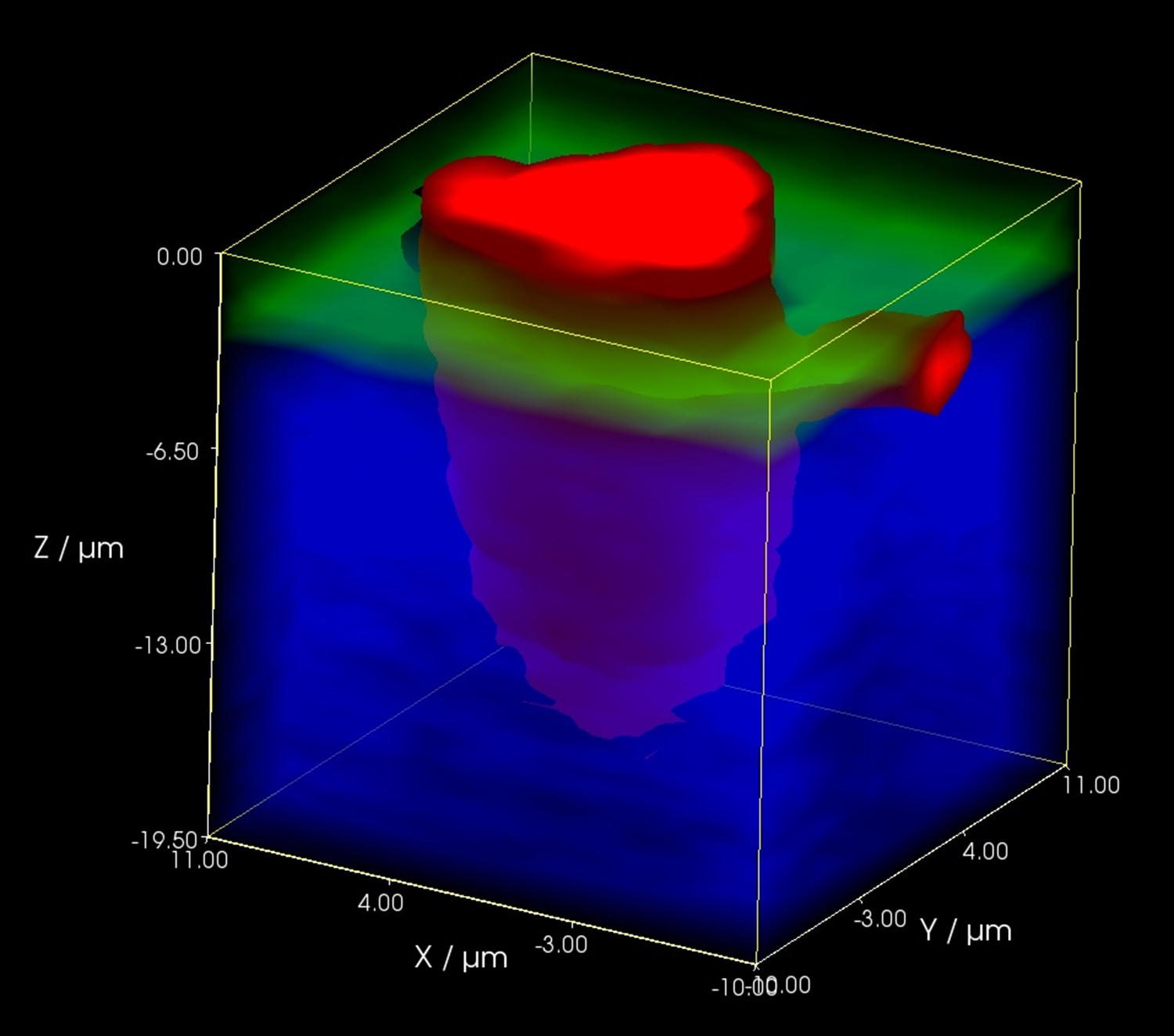
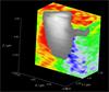
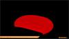
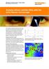
碳化硅晶片的3D拉曼成像
资料下载:材料科学(半导体材料)
-
 Application note: Photocurrent measurements on the inVia™ confocal Raman microscope [en]
When light interacts with semiconducting materials it can induce electrical currents (‘photocurrents’). These currents carry information about the electronic, optical, and charge transport properties of the material. This information is complementary to that obtainable from Raman scattering, which can identify physical changes in the material properties. This application note demonstrates the capability to simultaneously collect Raman and photocurrent data using the photocurrent mapping module concurrently with an inVia Raman microscope.
-
 Application note: Analyse compound semiconductors with the inVia™ Raman microscope [en]
Over the last decade compound semiconductors have attracted a great deal of attention because they offer properties suitable for next generation devices in a wide range of application areas. Historically, the fabrication of these devices has been hindered by material challenges. While these have mainly been conquered at the research level, problems still persist when scaling up to industrial production. Renishaw’s inVia Raman microscope is a non-invasive, non-destructive characterisation tool which provides sub-micrometre information on the vibrational, crystal and electronic structure of materials.
-
 Application note: Analyse silicon carbide (SiC) with the inVia Raman microscope [en]
The properties of silicon carbide are highly dependent on its crystal structure (it can exist in many polytypes), on the quality of the crystal, and on the number and types of defects present. Manufacturers of silicon carbide raw material and devices need to monitor and control these attributes to enhance yield. The first step in controlling these parameters is to measure them repeatably and quantifiably. Renishaw’s Raman systems are ideal for this.
-
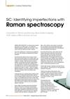 News release: Identifying imperfections with Raman spectroscopy [en]
An article in Compound Semiconductor magazine, October 2015, describes how Raman spectroscopy allows routine mapping of SiC wafers in little more than an hour.
相关新闻报道
Caltech借助inVia致力于解决全球能源问题
加州理工学院 (California Institute of Technology, Caltech) 正在做一个项目,即寻找一种仅通过阳光、水和二氧化碳来生产太阳能燃料的全新、有效的方法。他们重点研究光催化作用和光捕获。
雷尼绍inVia赢得2016年度“化合物半导体工业大奖”
工程技术领域的跨国公司荣幸宣布inVia显微拉曼光谱仪荣获2016年度测量类“化合物半导体工业大奖” (CS Industry Award)。由《化合物半导体》(Compound Semiconductor) 杂志组织举办的“化合物半导体工业大奖”是在www.compoundsemiconductor.net网站上通过投票评选出来的,覆盖整个化合物半导体行业。